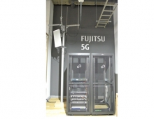
Fujitsu Achieves 56 Gbps Transmission Speeds In Wireless and Optical Connections
Fujitsu Laboratories and its partners have succeeded in achieving wireless transmission speeds of 56 Gigabits per second (Gbps) that can be used in trunk lines for future cellular base stations. The Japanese company has also developed the world's lowest power-consuming transceiver circuit that achieves communications speeds of 56 Gbps per channel. Working tith Tokyo Institute of Technology, Fujitsu Laboratories is trying to further enlarge the capacity of wireless equipment. The result of their reseach is a CMOS wireless transceiver chip that can process signals at high speeds with little loss across a broad range of frequencies, from 72 to 100 gigahertz (GHz). They also developed technology to modularize it. With these developments, they succeeded in achieving wireless transmission speeds of 56 Gigabits per second (Gbps), the world's fastest.
Currently, most networks that link base stations use optical fiber. However, t is difficult to expand service in areas where it is difficult to install a network of optical fiber cables, such as in urban areas or areas surrounded by rivers or mountains.
Tokyo Institute of Technology developed a technology for broadband, low-loss transceiver circuits in which data signals are split in two, with each converted to different frequency ranges, and then recombined. Each signal is modulated into a band 10-GHz wide, with the low-band occupying the 72-82 GHz range, and the high-band occupying the 89-99 GHz range. This technology enables modulation on an ultra-wideband signal of 20 GHz, with low noise and a similar range in the ratio between input and output power as existing 10 GHz band methods, which results in high-quality signal transmissions.
Tokyo Institute of Technology also developed an amplifier to send and receive as radio waves signals converted to the millimeter-waveband. The ultra-wideband amplifier for 72 to 100 GHz was designed with circuit technologies that stabilize the amplification ratio by feeding the amplitude of the output signal back to the input side for signal components whose amplification ratio decreases based on frequency.

The signal converted to the millimeter-waveband by the semiconductor chip is transported over the circuit board's signal path and supplied to the antenna. Because the antenna is made out of a waveguide (a metallic cylinder), there needs to be an ultra-wideband, low-loss connection between the printed circuit board and the waveguide. Fujitsu Laboratories and Tokyo Institute of Technology developed an interface between the circuit board and waveguide that uses a specially designed pattern of interconnects on the printed circuit board to adjust the impedance for the ultra-wideband range, enabling loss in the desired frequency range to be greatly reduced.
Indoor data-transfer tests were conducted, with two modules facing each other separated by a distance of 10 cm. These tests achieved data-transfer rates of 56 Gbps, the fastest wireless transmission speeds in the world, with loss of maximum 10% between the waveguide and circuit board.
By combining the technologies developed in this project with high-output amplifier technology, used to amplify the signal and increase the transport range, and baseband-circuit technology, used to process ultra-wideband signals, it is possible to increase the capacity of wireless equipment that can be installed outdoors.
Fujitsu Laboratories aims to have a commercial implementation of wireless trunk lines for cellular base stations around 2020.
The details of this technology will be announced at the IEEE International Solid-State Circuits Conference 2016 (ISSCC 2016), the largest conference related to semiconductor technology, opening in San Francisco on January 31 (ISSCC Presentation Number 13.3).
56 Gbps Transceiver Circuit for Optical Communications between Servers
Seperately, Fujitsu Laboratories Ltd. and Socionext Inc. have developed the world's lowest power-consuming transceiver circuit that achieves communications speeds of 56 Gbps per channel. Compared to previous levels, this essentially doubles the speed of data transfers between semiconductor chips, used in servers and switches, and optical modules.
Fujitsu Laboratories and Socionext have now developed a new timing detection method that combines the functions of the circuit that compensates signal degradation that becomes prominent as communication speeds improve with some of the functions of the timing-detection circuit that determines the bit-value of input signals, reducing the number of circuits. As a result, they succeeded in developing a 56 Gbps transceiver circuit that achieves twice the speed as before without raising power consumption.
This technology is able to increase the speed of data transfers between chips and optical modules without increasing power consumption, so it is expected to lead to performance improvements in next-generation servers and switches.
To reduce the power consumption of the CDR, Fujitsu Laboratories and Socionext have now developed a new timing error detection method. By analyzing waveforms after DFE calculation, Fujitsu Laboratories and Socionext discovered that they could detect whether the DFE's operational timing was early or late by comparing the results of the two DFE determination circuits in cases where three consecutive bits in the input signal were 100 or 011. This led them to develop a new timing detection method that only detects the timing when three consecutive bits of the incoming signal are 100 or 011.
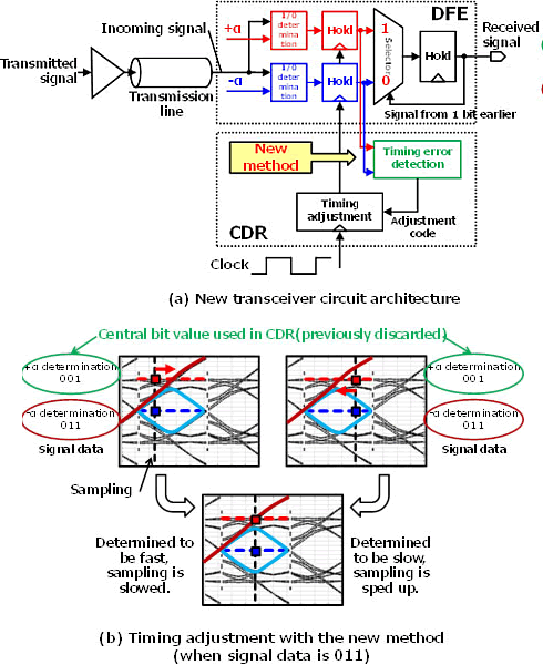
With this newly developed timing detection method, the two companies were able to eliminate the previously required CDR incoming-signal timing-determination circuit, and lines, such as the clock line, which were required as the DFE and CDR operated with different timing. This made it possible for them to succeed in developing transceiver circuitry that doubles speeds to 56 Gbps with the same power consumption as before.
Fujitsu Laboratories and Socionext will use the newly developed technology in interface components between optical modules and the chips of servers and switches, aiming for commercialization in fiscal 2018.