TSMC, GlobalFoundries/Samsung To Present Their 7nm Platforms At IEDM
TSMC will battle with the partnership of IBM, Globalfoundries and Samsung to detail rival 7nm processes at the International Electron Devices Meeting (IEDM) technical conference in December. IBM, Globalfoundries and Samsung have chosen to use extreme ultraviolet (EUV) light to pattern transistors, while TSMC's 7nm CMOS platform technology is expected to get to market first due to challenges getting EUV into production.
The 7nm FinFET technology to be disclosed by the IBM/Globalfoundries/Samsung technology development alliance is an integrated platform technology to use extreme ultraviolet (EUV) light to pattern transistors. A long-anticipated development, EUV lithography may become a requirement for ultra-small devices because the wavelength of EUV light is much shorter than that of the light currently used (13.5nm vs. 193nm) and it simplifies patterning.
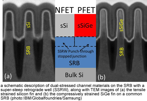
Using EUV, GF and Samsung claim that EUV lithography and other advanced patterning approaches have led to the tightest contacted polysilicon pitch (44/48nm) and metallization pitch (36nm) ever reported for FinFETs.
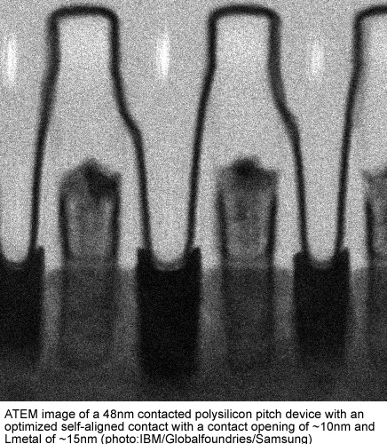
The pitches are smaller than the 56nm gate pitch Intel announced in August for its 10nm process, claiming industry-leading density for the node it aims to have in production next year.

According to the trio, their technology also features dual-strained channels on a thick strain-relaxed buffer (SRB) virtual substrate to combine tensile-strained NMOS and compressively strained SiGE PMOS for enhancement of drive current by 11% and 20%, respectively, versus a common planar HKMG process. It also features novel trench epitaxy to minimize the resistance of the highly scaled contact regions.
For its part, TSMC will describe at IEDM their 7nm CMOS platform technology for mobile system-on-a-chip (SoC) applications, featuring FinFET transistors. The technology can be optimized to emphasize either high performance or low power operation to accommodate the needs of diverse mobile applications. It features more than three times the gate density and either a speed gain (35-40%) or power reduction (>65%) versus the company’s commercial 16nm FinFET process. To demonstrate the technology, the researchers built a fully functional, low-voltage 256Mb SRAM test chip with full read/write functionality down to 0.5V, and the smallest SRAM cells ever reported (0.027µm2). Key features of the 7nm technology are an advanced patterning technique used with 193nm immersion lithography, an optimized fin width and profile, a raised source/drain epitaxial process that strains the transistor channel and reduces parasitics, a "novel" contact process, and a copper/low-k interconnect scheme featuring different metal pitches and stacks.

In September, GF said it developed its own 7nm process using immersion steppers that will be in production in 2018.
Earlier this week, Samsung announced its 10nm process, saying that it would skip a version of 7nm using today’s immersion lithography. Instead it said it will roll out 7nm with EUV targeting production before the end of 2018. TSMC said it will have limited production in 2017 for its 7nm process with immersion steppers.
Intel has yet to detail its 7nm node, but said it expects density to rise and cost per transistor to fall.
The IEDM papers suggest that TSMC and GF/Samsung could pull ahead of Intel, the long the leader in process technology.
TSMC managed to get orders for SoCs for Apple’s iPhone 7, in a blow for Samsung. The South Korean giant countered by grabbing much of TSMC’s business making competing Snapdragon chips from Qualcomm.
Intel has no stake in the mobile applications processors, although the company has won business making mobile SoCs for LG Electronics. Its core market for PC processors no longer demands rapid upgrades and it has a lead in the server market.
EUV still lags requirements of mass production in wafer throughput, defect density and reliability, issues could be ironed out in the next couple of years. In addition, EUV equipment is very expensive. The systems needed at or beyond the 7nm node will cost more than $100 million.
The 2016 IEEE International Electron Devices Meeting will be held in San Francisco, December 3-7.

