ABIT AN-8 Fatal1ty
4. Bios
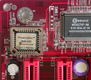
Abit BIOS was always one of my favourites. It was always complete and user friendly, and I was pleased to see that this hadn’t changed. The only negative thing is the VDIMM menu that doesn’t allow more than 2.8v. And even though this over voltage is more than enough for the majority of users, the more demanding and overclockers will certainly ask for more.
The available tweakings inside the OC Guru menu are:
-
VCore: 1.4v-1.75v
-
VDIMM: 2.5v-2.8v
-
DDR VTT: 1.25v-1.4v
-
DDR Ref Voltage: -60 to 0 to +60
-
CPU Ref Voltage: -60 to 0 to +60
-
Chipset Voltage: 1.5v-1.8v
-
HyperTransport Voltage: 1.2v-1.35v
-
LDT Multipliers: 1x-5x, AUTO
-
Memory Dividers: DDR400, DDR333, DDR266, DDR200
-
PCI-E Frequency: 100MHZ-145MHZ
-
HyperTransport Frequency (HTT): 200MHZ-410MHZ
-
CPU Multiplier: 4x-highest your CPU allows
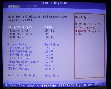
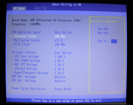
When we set the CPU operating speed to User Defined, various frequency related settings became accessible. The CPU maximum FSB can be only 410 MHz, but note that this setting also affects the memory and Hyper Transport bus speeds as well. The minimum option for the CPU multiplier is 4x, and the PCI Express bus speed is asynchronously set through the PCI E clock option. This option allows a maximum bus speed of 145MHz.
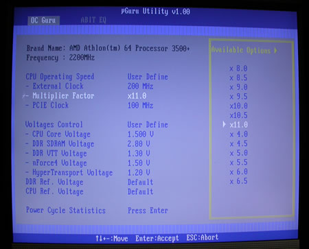
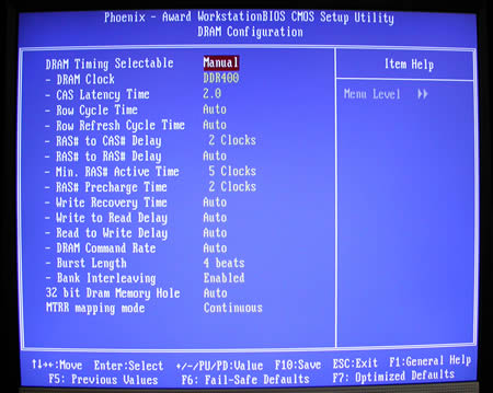
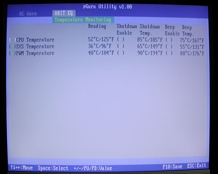
The nGuru utility menu is split in two individual sections, OC Guru and Abit EQ. OC Guru allows the manipulation of all board bus speeds and all board voltages, while the Abit EQ monitors all the voltages and the temperatures on the board.


The advanced Chipset Features menu contains various chipset related settings, such as the Hyper Transport and the memory settings.
From the HT Frequency Settings, we can actually control the speed of the Hyper Transport, with a maximum multiplier of 5x.
We also have the option to disable the SSE and SSE2 CPU registers, from the SSE / SSE2 menu option.

At the advanced Chipset Features, we find the memory controller settings that offer a wide variety of settings, where you can manually configure the RAS to CAS delay, row to row delay which is shown as RAS to RAS Delay, active to precharge delay shown as Min RAS Active Time, RAS precharge delay; write recovery time, write to read delay, read to write delay, command rate, burst length, and memory register access and cacheability shown as MTRR Mapping Mode. Also available is the ability to adjust a lot of secondary parameters for the memory subsystem.
