Fujitsu's Technology Paves The Way For Commercialization of MRAM
Fujitsu Laboratories Limited today announced the development of a new memory cell circuit for spin-torque-transfer MRAM that enable a space savings of 60% and achieve a greater degree of integration than was previously possible.
Spin-torque-transfer MRAM is regarded as a next-generation non-volatile memory with high potential to become a replacement for NOR-type flash memory, since its compact in size, consumes less power and offers higher performance.
Currently, microcontrollers for mobile phones and PDAs typically employ NOR-type flash memory, which is approaching its physical limits of miniaturization - however, there is continuous demand for further miniaturization of such non-volatile memory for microcontrollers in handheld electronic devices, as the devices continually become smaller. As a result, spin-torque-transfer MRAM has gained a great deal of attention as a potential successor to NOR-type flash memory, as spin-torque-transfer MRAM can conserve space, and there has been a significant amount of research aimed at its practical implementation. Fujitsu's new technology was used to reduce the area of memory cell circuits by 60%, thus enabling a higher degree of integration unattainable with previous spin-torque-transfer MRAMs, resolving one of the technology's key technical implementation challenges for practical use. As a result, the technology paves the way for microcontrollers embedded with spin- torque-transfer MRAM that are more compact, and which can run applications more quickly than microcontrollers embedded with NOR-type flash memory.
Details of the novel technology will be presented at the 2010 Symposium on VLSI Technology (2010 VLSI), held in Honolulu, U.S. from June 15-17 (Presentation number: 5.2).
Background
Spin-torque-transfer MRAM is a memory storage element that makes use of the phenomenon in which passing a current through a magnetic material causes its direction of magnetization to reverse. Passing a current through the material causes the direction of magnetization to either be in a parallel or anti-parallel state. This high or low electrical resistance can be handled in terms of binary digital information, either 1 or 0, enabling the storage element to be used as non-volatile magnetic memory (Figure 1).

While it has been possible to miniaturize MTJ elements used in spin-torque-transfer MRAM, shrinking the adjoining cell-select transistors had thus far posed a challenge.
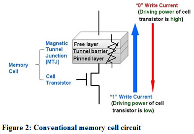
The memory cell circuit in spin-torque-transfer MRAM is a circuit that connects the MTJ element with a cell-select transistor, which act as switches that select which MTJ elements to write to or read from. With existing memory cell circuits, when the MTJ element of a spin-torque-transfer MRAM has been written to a high-resistance state ("1"), voltage is lowered through variable resistance - this requires a larger current to write than when an MTJ element it is switched to a low resistance state ("0"), which is not affected by variable resistance. In other words, because the cell-select transistor's current-driving capability is low, writing to a high-resistance state ("1") would require a significant current. As such, even with a low driving-current capability, cell-select transistors need to be relatively large to ensure an adequate write current, which has been a barrier to reducing transistor size.
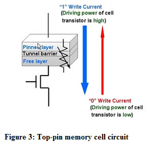
Fujitsu Laboratories has reversed the order of the MTJ element's magnetic layers, enabling the development of a new MTJ element with a top-pinned structure - that differs from previous structures - that consists of a pinned layer, tunnel barrier, and free layer. However, because the distance between the tunnel barrier of the top-pinned MTJ element and its bottom electrode has been reduced, electrical short failures are more likely to occur during fabrication - as a countermeasure to address this issue, Fujitsu Laboratories has inserted a buffer layer to maintain separation between the tunnel barrier and bottom electrode, which allows the output from the low-resistance ("0") writing to travel in the same direction as the cell-select transistor's low driving-current capacity, thus making it possible for the cell-select transistor to still function at a smaller size.

Currently, microcontrollers for mobile phones and PDAs typically employ NOR-type flash memory, which is approaching its physical limits of miniaturization - however, there is continuous demand for further miniaturization of such non-volatile memory for microcontrollers in handheld electronic devices, as the devices continually become smaller. As a result, spin-torque-transfer MRAM has gained a great deal of attention as a potential successor to NOR-type flash memory, as spin-torque-transfer MRAM can conserve space, and there has been a significant amount of research aimed at its practical implementation. Fujitsu's new technology was used to reduce the area of memory cell circuits by 60%, thus enabling a higher degree of integration unattainable with previous spin-torque-transfer MRAMs, resolving one of the technology's key technical implementation challenges for practical use. As a result, the technology paves the way for microcontrollers embedded with spin- torque-transfer MRAM that are more compact, and which can run applications more quickly than microcontrollers embedded with NOR-type flash memory.
Details of the novel technology will be presented at the 2010 Symposium on VLSI Technology (2010 VLSI), held in Honolulu, U.S. from June 15-17 (Presentation number: 5.2).
Background
Spin-torque-transfer MRAM is a memory storage element that makes use of the phenomenon in which passing a current through a magnetic material causes its direction of magnetization to reverse. Passing a current through the material causes the direction of magnetization to either be in a parallel or anti-parallel state. This high or low electrical resistance can be handled in terms of binary digital information, either 1 or 0, enabling the storage element to be used as non-volatile magnetic memory (Figure 1).

While it has been possible to miniaturize MTJ elements used in spin-torque-transfer MRAM, shrinking the adjoining cell-select transistors had thus far posed a challenge.
The memory cell circuit in spin-torque-transfer MRAM is a circuit that connects the MTJ element with a cell-select transistor, which act as switches that select which MTJ elements to write to or read from. With existing memory cell circuits, when the MTJ element of a spin-torque-transfer MRAM has been written to a high-resistance state ("1"), voltage is lowered through variable resistance - this requires a larger current to write than when an MTJ element it is switched to a low resistance state ("0"), which is not affected by variable resistance. In other words, because the cell-select transistor's current-driving capability is low, writing to a high-resistance state ("1") would require a significant current. As such, even with a low driving-current capability, cell-select transistors need to be relatively large to ensure an adequate write current, which has been a barrier to reducing transistor size.

Fujitsu Laboratories has reversed the order of the MTJ element's magnetic layers, enabling the development of a new MTJ element with a top-pinned structure - that differs from previous structures - that consists of a pinned layer, tunnel barrier, and free layer. However, because the distance between the tunnel barrier of the top-pinned MTJ element and its bottom electrode has been reduced, electrical short failures are more likely to occur during fabrication - as a countermeasure to address this issue, Fujitsu Laboratories has inserted a buffer layer to maintain separation between the tunnel barrier and bottom electrode, which allows the output from the low-resistance ("0") writing to travel in the same direction as the cell-select transistor's low driving-current capacity, thus making it possible for the cell-select transistor to still function at a smaller size.
