Samsung Debuts 7nm LPP EUV, SmartSSD and 256GB 3DS RDIMM at Samsung Tech Day
Samsung Electronics today announced several additions to its semiconductor ecosystem that encompass next-generation technologies in foundry as well as NAND flash, SSD (solid state drive) and DRAM.
Unveiled at its annual Samsung Tech Day include:
- 7nm EUV process node from Samsung's Foundry Business, providing significant strides forward in power, performance and area.
- SmartSSD, a field programmable gate array (FPGA) SSD, that will offer accelerated data processing and the ability to bypass server CPU limits.
- QLC-SSD for enterprise and datacenters that offer 33-percent more storage per cell than TLC-SSD, consolidating of storage footprints and improving total cost of ownership (TCO).
- 256-gigabyte (GB) 3DS (3-dimensional stacking) RDIMM (registered dual in-line memory module), based on 10nm-class 16-gigabit (Gb) DDR4 DRAM that will double current maximum capacity to deliver higher performance and lower power consumption.
7nm EUV
"Bringing 7nm EUV into production is an incredible achievement. Also, the announcements of SmartSSD and 256GB 3DS RDIMM represent performance and capacity breakthroughs that will continue to push compute boundaries. Together, these additions to Samsung's comprehensive technology ecosystem will power the next generation of datacenters, high-performance computing (HPC), enterprise, artificial intelligence (AI) and emerging applications," said said JS Choi, President, Samsung Semiconductor, Inc.

Initial wafer production of Samsung's 7nm LPP (Low Power Plus) EUV process node represents a milestone in semiconductor fabrication. Samsung said that it has taped out and is ramping multiple 7nm chips using EUV following a similar announcement earlier this month from its larger foundry rival TSMC.
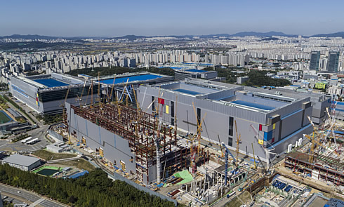
Samsung's research and development in EUV began in the 2000s. The initial EUV production has started in Samsung's S3 Fab in Hwaseong, Korea.
EUV systems supported 250-W light sources on a sustained basis since early this year at Samsung's S3 fab in Hwaseong, South Korea. The power level drove throughput up to the needed 1,500 wafers/day for production. Since then, EUV systems have hit a peak 280 W, and Samsung targets 300 W.
EUV uses 13.5nm wavelength light to expose silicon wafers as opposed to conventional argon fluoride (ArF) immersion technologies that are only able to achieve 193nm wavelengths and require expensive multi-patterning mask sets. EUV enables the use of a single mask to create a silicon wafer layer where ArF can require up to 4 masks to create that same layer. EUV eliminates a fifth of masks required with traditional argon-fluoride systems, raising yields. However, the node still requires some multi-patterning in base layers at the front-end-of-line. Consequently Samsung's 7LPP process can reduce the total number of masks by about 20% compared to non-EUV process.
Samsung has also developed proprietary capabilities such as a unique mask inspection tool that performs early defect detection in EUV masks, allowing those defects to be eliminated early in the manufacturing cycle.
The EUV lithography improvements also deliver increased performance, lower power and smaller area while improving design productivity by reducing mulit-patterning complexity. Compared to its 10nm FinFET predecessors, Samsung's 7LPP technology not only greatly reduces the process complexity with fewer layers and better yields, but also delivers up to a 40% increase in area efficiency with 20% higher performance or up to 50% lower power consumption.

By 2020, Samsung expects to secure additional capacity with a new EUV line for customers who need high-volume manufacturing for next-generation chip designs.
Samsung complements the production of its 7nm EUV with SAFE ecosystem solutions.
In conjunction with key Samsung Advanced Foundry Ecosystem (SAFE) partners, Samsung's customers can now rely on a set of design collaterals to embark on Samsung's new process node technology. Specifically, SAFE partners - Ansys, Arm, Cadence, Mentor, SEMCO, Synopsys and VeriSilicon - have enabled Process Design Kits (PDK), IP, Reference Flows, Advanced Packaging Solutions and Design Services.
From high-performance and high-density embedded memories and logic libraries to the most advanced interface IP solutions including HBM2/2E, GDDR6, DDR5, USB 3.1, PCI Express 5.0 and 112G SerDes, SAFE is ready to help customers implement their designs on 7LPP EUV. Early design kits (DK) are now available.
SAFE is also prepared for Samsung's customers to begin their designs today using fully certified PDK tools and reference flows from Samsung's partners at ANSYS, Cadence, Mentor and Synopsys. These partner tools and flows have been fully qualified on the new 7LPP EUV process technology and are ready today.
Advanced packaging plays a larger role in the design ecosystem. SAFE is ready to complement the complex customer designs on 7LPP EUV with a full range of advanced packaging solutions including 2.5D silicon interposer and new innovations like Embedded Passive Substrates.

For 7LPP EUV, SAFE is also enabled with a complete range of design services from Samsung's partners like VeriSilicon.
Both Samsung and TSMC will apply EUV probably only to two chip layers at 7nm, so far not using protective pellicles that are still in development. They will extend EUV to perhaps six layers at 5nm nodes, but that may not come until 2021, when pellicles will have sufficient durability and light-transmission capabilities.
Samsung is probably six months ahead with an EUV process because they have been using the systems with DRAM and logic, but TSMC is way ahead in enablement with IP and tools and is working with more customers such as AMD, Apple, HiSilicon, and Nvidia, among others.
Qualcomm is expected to split its 7nm work between TSMC and Samsung.
Samsung is also on track to start production of 5- and 4nm nodes before June, providing evolutionary improvements with the same device sets. PDKs for the nodes could be released before the end of the year, and a second shell for EUV production is being built next to the S3 fab.
The three nodes will move the contact closer to and eventually over the gate to increase density and reduce metal pitches. It's an approach that Intel previously discussed for its 10nm node that is still not in volume production.
Samsung announced in May its plans to move to gate-all-around transistors, also described as nanosheets, for a 3nm node. It aims to drop nominal voltage to a new low to continue power savings. The first cut of a version 0.1 PDK for a 3nm node could be available by June.
Core Memory business
Samsung also enables advanced providers of server-less computing through products including the new SmartSSD, quad-level cell (QLC)-SSD, 256GB 3DS RDIMM as well as High Bandwidth Memory (HBM) 2 Aquabolt. By accelerating data processing, bypassing server CPU limits and reducing power demands, these products will enable datacenter operators to continue to scale at faster speeds while containing costs.
Samsung's flash memory products for future datacenters will also include Key Value (KV)-SSD and Z-SSD. KV-SSD eliminates block storage inefficiency, reducing latency and allowing datacenter performance to scale evenly when CPU architectures max out. The company's next-generation Z-SSD will be the fastest flash memory ever introduced, with dual port high availability, ultra-low latency and a U.2 form factor, designed to meet the emerging needs of enterprise clients. Z-SSD will also feature a PCIe Gen 4 interface with a blazing-fast 12-gigabytes-per-second (GB/s) sequential read, which is 20 times faster than today's SATA SSD drives.
A range of Samsung solutions will enable the development of upcoming machine learning and AI technologies. The Tech Day AI display highlighted astounding data transfer speeds of 16Gb GDDR6 (64GB/s), ultra-low latency of Z-SSD and performance of Aquabolt, which is the highest of any DRAM-based memory solution currently in the market.
Enterprise products on display at Tech Day included D1Y 8Gb DDR4 Server DRAM, which incorporates the most advanced DRAM process, resulting in lower power usage.
Samsung said that it is sampling 256-GByte RDIMMs made with its 16-Gbit chips. The cards, running at DDR4 speeds up to 3,200 MHz and supporting 50-ns reads and writes, should be in production before the end of the year.
The chips are made in a 1y-nm process. It was not clear whether EUV is being applied to the 1y process. However, follow-on 1z and 1a nodes will increasingly use EUV.
Samsung showed eight of the DIMMs running on an AMD Epyc server. They hit 3.2 million operations/second at 170 W compared to its existing 128-GB cards delivering 3.8 million ops/s at 225 W.
Ultimately, Samsung aims to boost DIMMs to 768 GBytes. It also aims to raise HBM data rates to 512 GB/s from 307 GB/s today. GDDR6 graphics memories will hit 22 Gbits/s from 18 Gbits/s today, and LPDDR memories will fall from 24 mW/GB to 12 mW/GB, he added, without providing time frames.
Additionally, Samsung's dual-port x4 PCIe Gen 4 32TB SSD offers 10GB/s performance. Samsung's 1Tb QLC-SSD presents a cutting-edge storage option for enterprise clients with competitive efficiency when compared to hard disk drives (HDD), while KV-SSD allows server performance to scale even as CPU architectures max out, also providing a competitive TCO, write amplification factor (WAF) improvement and scalability.
Samsung's QLC-SSD, Z-SSD and 8GB Aquabolt help high-performance computing clients blast through performance barriers and reach new heights. The 8GB Aquabolt provides the fastest data transmission speed and highest performance of any DRAM-based memory solution on the market today at 307GB/s per HBM cube. QLC-SSD and Z-SSD are also offered in a tiered storage solution that results in a 53-percent increase in overall system performance.
Samsung also announced plans for smart solid-state drives (SSDs) using embedded Xilinx Zynq FPGAs to bolster performance 2.8x to 3.3x. The SmartSSDs target a wide range of database, AI, video, and storage applications.
The SSDs will provide an easier way to scale performance than matching banks of standard FPGAs to separate accelerators, said the company. The products, still in a prototype phase, will use a range of densities and medium-grade FPGAs.


