Toshiba develops Silicon Nanowire Transistor for 16nm Generation and Beyond
Toshiba has developed a breakthrough technology for a nanowire transistor, a major candidate for a 3D structure transistor for system LSI in the 16nm generation and beyond.
The company has achieved a 1mA/μm on-current, the world's highest level for a nanowire transistor, by reducing parasitic resistance and improving the on-current level by 75%. This is a major step towards practical application of nanowire transistors. This achievement will be presented at the 2010 Symposium on VLSI Technology in Hawaii, on June 17.
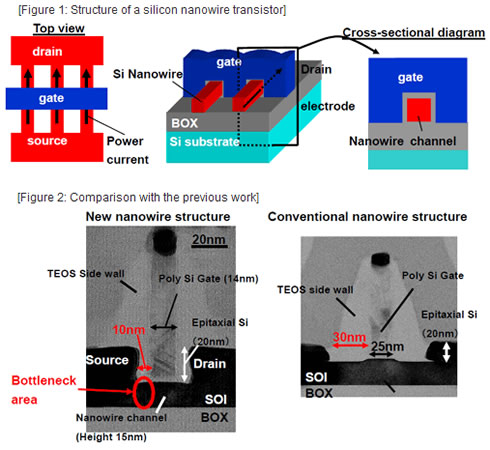
When the size of current planar transistors scales smaller, current leakage between the source and the drain at its off-stage (off-leakage) will become a critical problem in securing circuit reliability. To overcome this, transistors with a 3D structure, including silicon nanowire transistors, are being investigated as candidates for future generations of devices. The silicon nanowire transistor can suppress off-leakage and achieve further short-channel operation, because its thin wire-shaped silicon channel (nanowire channel) is effectively controlled by the surrounding gate. However, parasitic resistance in the nanowire-shaped source/drain, especially in the region under the gate sidewall, degrades the on-current.
Toshiba overcame this problem by optimizing gate fabrication and significantly reducing the thickness of the gate sidewall, from 30nm to 10nm. Low parasitic resistance was realized by epitaxial silicon growth on the source/drain with a thin gate sidewall, which leads to a 40% increase in on-current. The company also achieved a further 25% increase in current performance by changing the direction of the silicon nanowire channel from the to plane direction. Utilizing these technologies, Toshiba has demonstrated an on-current level of 1mA/μm, when the off-current is 100nA/μm, a 75% increase in the on-current at the same off-current condition.
Toshiba's work was partly supported by New Energy and Industrial Technology Development Organization (NEDO) 's Development of Nanoelectronic Device Technology.


