Epson and Fujitsu Announce Results of Joint Project to Develop FRAM Technology
Epson and Fujitsu announced the results of their joint project to develop next-generation Ferroelectric Random Access Memory (FRAM) technology.
Since announcing a joint development agreement in June 2005, Epson
and Fujitsu have collaborated on development of next-generation
technology for FRAM non-volatile memory. FRAM is a non-volatile memory that uses a ferroelectric film as the capacitor for data retention. The joint development
project was successfully completed recently and produced the
anticipated results.
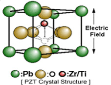 Through the project, the two companies developed technology for
forming, processing and evaluating a new ferroelectric (PZT) film
and created FRAM memory core process technology that is highly
integrated (four times the level of conventional FRAM), features
high performance (read/write speeds over three times faster than
conventional FRAM) and boasts high reliability (capable of
more than one hundred trillion read/write cycles). FRAM is currently
attracting attention as a cutting-edge technology for secure memory,
and this level of performance is a world first. Since the
ferroelectric process can be added to existing CMOS logic processes,
it will be suitable for the development of mass production
technologies.
Epson intends to combine the results of this joint project with its own low power consumption CMOS technology to further speed up development and commercialization of integrated large-scale integrated circuits (LSIs) for applications such as battery-operated and portable devices.
Fujitsu will proceed with development of mass production technologies based on the results of this joint project.


