Cadence Announces Tapeout of GDDR6 IP on Samsung's 7LPP Process
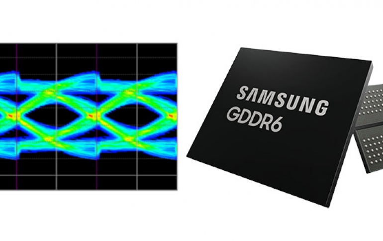
Cadence Design Systems, Inc. today announced the tapeout of a complete GDDR6 memory IP solution on Samsung’s 7LPP process.
GDDR6 memory is targeted at very high-bandwidth applications including machine learning, AI, cryptocurrency mining, graphics, automated driving, ADAS and high-performance computing (HPC). The Cadence GDDR6 IP solution consists of PHY, controller and Verification IP (VIP). Samsung is enabling this advanced IP on the 7LPP foundry process for next-generation chips for use with high-performance GDDR6 memory product, and not only graphics applications.
Until recently, DDR4 and LPDDR4 have been the memories of choice for early adopters addressing high-bandwidth memory applications. GDDR6 offers 5X faster memory bandwidth than the fastest speed of DDR4 at a moderate cost, making it a good choice for such applications. However, design at GDDR6 data rates requires new architecture and techniques, which has limited the adoption of GDDR technology in non-graphics applications in the past. Samsung and Cadence are poised to address this market need with GDDR6 solutions that include the Cadence Denali DDR controller and high-speed SerDes technology.
The new GDDR6 IP allows up to 16Gb/sec bandwidth per pin, or over 500Gb/sec peak bandwidth between the SoC and each GDDR6 memory die. This enables users to design high-memory-bandwidth GDDR6 interfaces with a lower number of DRAM dies than is possible with DDR4, reducing both PCB area and packaging pins.
Cadence’s GDDR6 controller is based on the company's DDRx and LPDDRx controllers. Integrating popular and silicon-proven DRAM controller features like Arm AMBA AXI ports, multiport arbitration, a priority-based and bandwidth-based reordering queue, RAS features, memory BIST, and in-line ECC, the goal of Cadence’s GDDR6 controller is to give the user the same facilities they are used to with DDR and LPDDR controllers while connecting to GDDR6.
Cadence’s GDDR6 controller is pipelined correctly and geared for implementation to connect to a DFI interface modified for GDDR6 with low latency, while closing timing at 16G speeds and above in 7nm technologies.
Additional Features of the Cadence GDDR6 IP:
- Cadence design techniques reuse technology from Cadence’s DDR and SerDes designs, resulting in lower risk when implementing GDDR6
- Low bit-error rate (BER) reduces retries on the memory bus, providing greater bandwidth and lower maximum latency
- Cadence’s wide design margin allows users to implement GDDR6 on PCBs with common materials such as FR4, reducing the cost of GDDR6 deployment
- Cadence’s GDDR6 reference design allows users to replicate Cadence’s test chip results in their own products
- Cadence’s VIP, now extended with GDDR6 support
Cadence GDDR6 IP and memory models are available now. Ccadence is offering design files to select customers to begin integration work.


